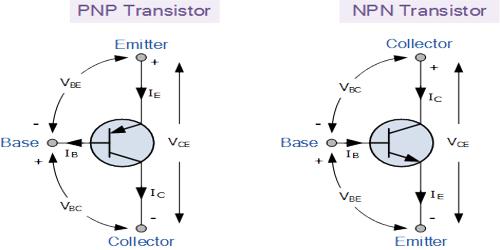
Working Principle of n-p-n transistor
N-P-N Transistors are three-terminal, three-layer devices that can function as either amplifiers or electronic switches. Here working principle of a “n-p-n transistor” is explained. It is made up of three semiconductor layers: one p-type semiconductor layer and two n-type semiconductor layers.
In figure (a) and (b) electric circuits of a “n-p-n transistor” have been shown. The emitter-base junction, in the left of the figure, has been kept in forward bias. So, n-region is more positive than p region. As a result electrons from is-region can easily come to the p region. That means, electrons from the emitter come to the base. Hence emitter current IE is produced. As electrons enter into the p-type base region so holes in that region intend to combine. But since the base is very thin only a small amount of electrons (about 5%) combine with holes and generate base current IB.
![]()
Base-collector junction in the right is kept in reverse bias hence collector region becomes more positive and electrons coming to the base from the emitter is speeded to the n-region. That means n-region or collector collects electrons. While coming through the base some electrons are combined with holes, but about 95% electrons move to the collector region and collector current IC from base to collector is produced. For a very small number of electrons combine with holes in the base region to the base region is made very thin so that presence of electrons here becomes short and lightly doped so that number of holes becomes less.
In this way, almost total emitter current flows to the collector. So, it is seen that emitter current is the summation of base current and collector current. That means,
IE = IB + IC