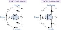
Junction Diode: Construction and Working Principle
Construction: If a p-type and n-type semiconductors are connected by a special technique then the junction surface is called a p-n junction. It is one of the simplest semiconductor devices around, and which has the characteristic of passing current in only one direction only. One part of a pure semiconductor crystal is made p-type and the other part n-type by doping impurities in a controlled way at high temperature and the p-n junction is made.
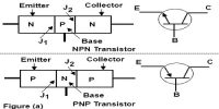
The surface of a p-n junction which is in the p-type region has a majority carrier’s holes and the surface which is in the n-type region has majority carrier’s electrons. When p-type and n-type regions are connected then electrons of the n-type region are attracted by the holes of the p-region and move to the junction by the diffusion process. Similarly holes from the p-region move to the junction being attracted by the electron of n [Fig. (a)].
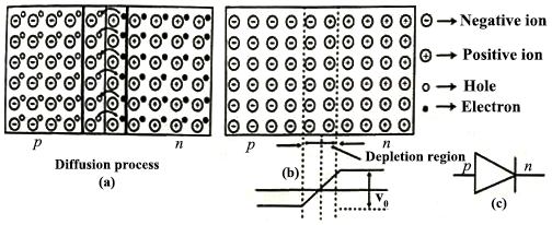
In the p-n junction, both holes and electrons combine and become neutral. The atom from which electron in the it-type region that move to the junction becomes positive ion and the atom from where the hole in the p-region move to the junction becomes negative ion [Fig. (a)]. Symbol of the p-n junction has been shown in [Fig. (c)].
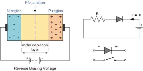
Now holes coming from p-region are repelled by positive ions and electrons from n-region are repelled by negative ions. In this way, a small depletion region or a thin layer is produced. The width of this region or layer is from 10-6 m to 10-8 m. In two sides of the junction, a thin layer keeps positive and negative charges separated where the moving charge becomes exhausted and no moving charge carriers are available. This layer or region is called depletion layer or region. In the figure, a diffusion process and depletion region are shown.
This depletion region is called a junction barrier. In this junction, a small potential difference is produced. Hence, this region is sometimes called potential difference region or potential difference barrier. Its value is normally from 01 to 0-3 V. From the figure (b) it is clear that the potential difference barrier V0 creates an electric field which creates resistance to the majority carriers to cross their individual region. In this way p-n semiconducting crystal being connected from junction diode (abbreviated as a diode).