Carbon-based nanomaterials’ properties can be altered and engineered by purposefully introducing structural “imperfections” or defects. The challenge, however, is to keep the number and type of defects under control.
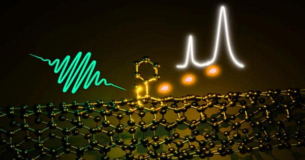
In the case of carbon nanotubes – microscopically small tubular compounds that emit near-infrared light – chemists and materials scientists at Heidelberg University led by Prof. Dr. Jana Zaumseil have now demonstrated a new reaction pathway that allows for such defect control. It produces specific optically active defects, known as sp3 defects, that are more luminescent and can emit single photons, or light particles. Near-infrared light emission efficiency is critical for applications such as telecommunications and biological imaging.
Optically Active Defects Improve Carbon Nanotubes. Prof. Dr Jana Zaumseil have now demonstrated a new reaction pathway to enable such defect control.
Chemists and materials scientists have now demonstrated a new reaction pathway for carbon nanotube control. It produces optically active sp3 defects that are more luminescent and capable of emitting single photons in the near-infrared.
Defects are typically regarded as something “bad” that has a negative impact on the properties of a material, making it less perfect. However, in some nanomaterials, such as carbon nanotubes, these “imperfections” can result in something “good” and allow for new functionalities. The precise type of defect is critical in this case. Carbon nanotubes are made up of rolled-up sheets of a hexagonal lattice of sp2 carbon atoms, just like benzene. These hollow tubes have a diameter of about one nanometer and can be several micrometers long.
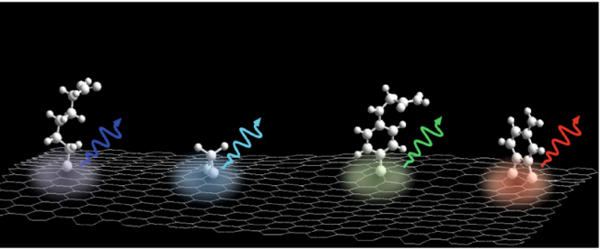
Certain chemical reactions can convert a few sp2 carbon atoms in the lattice to sp3 carbon, which is also found in methane and diamond. This alters the local electronic structure of the carbon nanotube, resulting in an optically active defect. These sp3 defects emit light even further in the near-infrared and are thus more luminescent than unfunctionalized nanotubes. Because of the geometry of carbon nanotubes, the precise position of the introduced sp3 carbon atoms determines the optical properties of the defects.
“Unfortunately, so far there has been very little control over what defects are formed,” says Jana Zaumseil, who is a professor at the Institute for Physical Chemistry and a member of the Centre for Advanced Materials at Heidelberg University.
The Heidelberg researcher and her colleagues recently demonstrated a new chemical reaction pathway that allows for defect control and the selective creation of only one type of sp3 defect. These optically active flaws are “better” than any of the previous “imperfections.” Prof. Zaumseil explains that they are not only more luminescent, but they also emit single photons at room temperature. Only one photon is emitted at a time in this process, which is required for quantum cryptography and highly secure telecommunication.
This new functionalisation method – a nucleophilic addition – is very simple and does not require any special equipment, according to Simon Settele, a doctoral student in Prof. Zaumseil’s research group and the first author on the paper reporting these results. “We are only now beginning to investigate the potential applications. Many aspects of chemistry and photophysics are still unknown. The goal, however, is to create even better defects.”
This study is part of Prof. Zaumseil’s project “Trions and sp3-Defects in Single-walled Carbon Nanotubes for Optoelectronics” (TRIFECTs), which is funded by an ERC Consolidator Grant from the European Research Council (ERC). Its goal is to comprehend and engineer the electronic and optical properties of carbon nanotube defects.
“The chemical differences between these defects are subtle, and the desired binding configuration is typically only formed in a small percentage of nanotubes.” The ability to produce large numbers of nanotubes with a specific defect and with controlled defect densities paves the way for optoelectronic devices and electrically pumped single-photon sources, which are required for future applications in quantum cryptography, according to Prof. Zaumseil.